
mPCIe with user programmable Artix-7 FPGA, AD/DA, DIO channe
SKU:
TMPE627
Fabrikant:
Tews
- I/O Type : Analog I/O
- Bus Type : mPCIe
Tews Reconfigurable FPGA with AD/DA & Digital I/O PCIe Mini Card
Details
More Information
Downloads
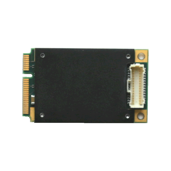
Tews mPCIe module with Xilinx XC7A50T-2 FPGA
The TMPE627 is a standard full PCI Express Mini Card, providing a user programmable Xilinx Artix-7 7A50T FPGA.The TMPE627 provides 14 ESD-protected 5 V-tolerant TTL lines. All I/O lines are individually programmable as input or output. TTL I/O lines can be set to high, low, or tristate. Each TTL I/O line has a pull-resistor to a common programmable pull-up voltage that can be set so +3.3 V, +5 V and GND.
The 16 bit ADC offers 4 input channels that can be software configured to operate in single-ended or differential mode. It offers software selectable input voltage ranges of 0-5.12 V, 0-10 V, 0-10.24 V, ±5 V, ±5.12 V, ±10 V and ±10.24 V with a sampling rate of up to 200 ksps.
The DAC offers 4 channels of 16 bit analog outputs with software selectable output voltage ranges of 0-5 V, 0-10 V, 0-10.8 V, ±5 V, ±10 V or ±10.8 V. The output voltage range can be individually set per channel. The conversion time is typ. 10 µs and the DAC outputs are capable to drive a load of 2 Kohm, with a capacitance up to 4000 pF.
Each TMPE627 is factory calibrated. The calibration information is stored in an on board serial EEPROM unique to each TMPE627 module.
The I/O signals are accessible through a 30 pin Pico-Clasp latching connector.
The User FPGA is configured by a SPI flash. An in-circuit debugging option is available via a JTAG header for read back and real-time debugging of the FPGA design (using the Vivado ILA). With the TA308 Programming Kit direct JTAG access to the FPGA is possible, using the Xilinx Platform Cable USB.
User applications for the TMPE627 with 7A50T FPGA can be developed using the design software Vivado Design Suite HL WebPACK Edition, which can be downloaded free of charge from www.xilinx.com.
TEWS offers a well-documented basic FPGA Example Application design. It includes a constraints file with all necessary pin assignments and basic timing constraints. The example design covers the main functionalities of the TMPE627. It implements PCIe to register mapping and basic I/O. It comes as a Xilinx Vivado Design Suite project with source code and as a ready-to-download bit stream.
|
|